A seismic shift has irrevocably altered the landscape of modern computing. For decades, the Central Processing Unit (CPU) reigned supreme, but a dramatic and historic transition is now undeniable: Graphics Processing Units (GPUs) have ascended as the dominant force in accelerated computing. At the heart of this profound transformation stands NVIDIA, a company that has not merely adapted to change but has actively architected a new era of AI and supercomputing. This shift is reshaping every facet of the tech world, from scientific discovery and enterprise data centers to, perhaps most intimately for our readers, the very core of gaming technology.
The Genesis of GPU Power: From Graphics to General Purpose
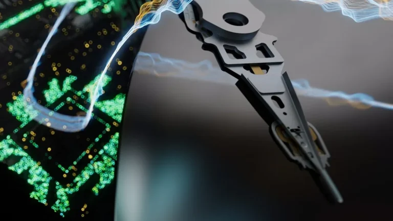
NVIDIA’s journey to this apex of computing began with a series of audacious strategic decisions, none more illustrative than the ‘bet-the-company’ moment with the RIVA 128. Faced with dwindling resources and fierce competition in the nascent 3D graphics market, NVIDIA CEO Jensen Huang famously pushed his team to create the world’s first fully hardware-accelerated 3D pipeline, commissioning production sight unseen after extensive, painstaking simulation. This intense focus on optimizing graphics, initially for gaming, unexpectedly laid the crucial groundwork for general-purpose GPU (GPGPU) computing. The subsequent visionary investment in CUDA, NVIDIA’s proprietary parallel computing platform, further cemented this path. While traditional CPUs struggled with inherently serial processing, GPUs, with their massive parallel architectures, were uniquely suited to simultaneously handle thousands of threads, a capability that would later prove indispensable for the explosion of AI and machine learning.
“I knew it’s going to be perfect, because if it’s not, we’ll be out of business. So let’s make it perfect. We get one shot.”
— Jensen Huang on RIVA 128
NVIDIA’s Full-Stack Ecosystem: Hardware, Software, Interconnects
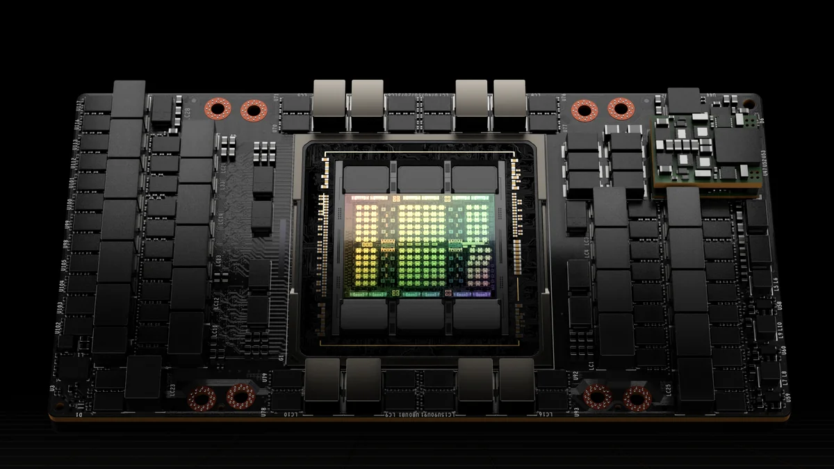
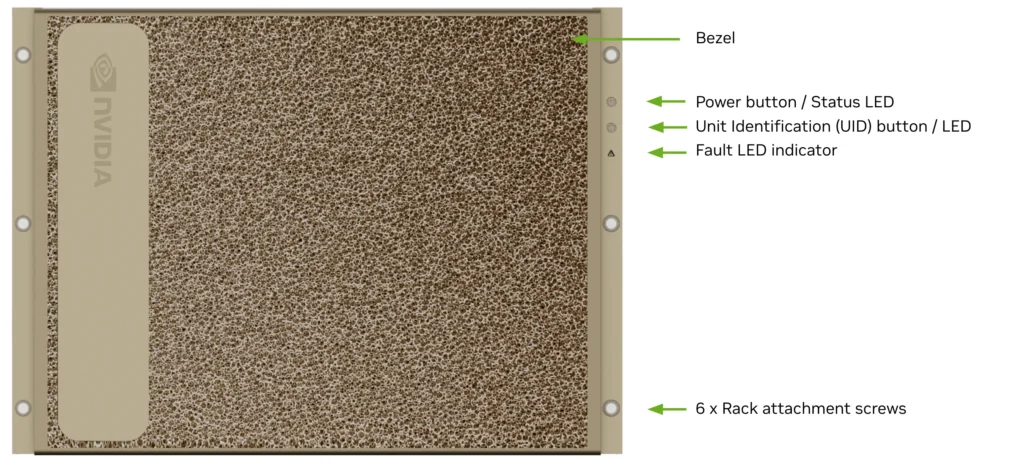
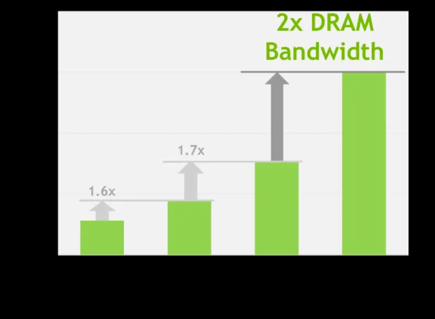
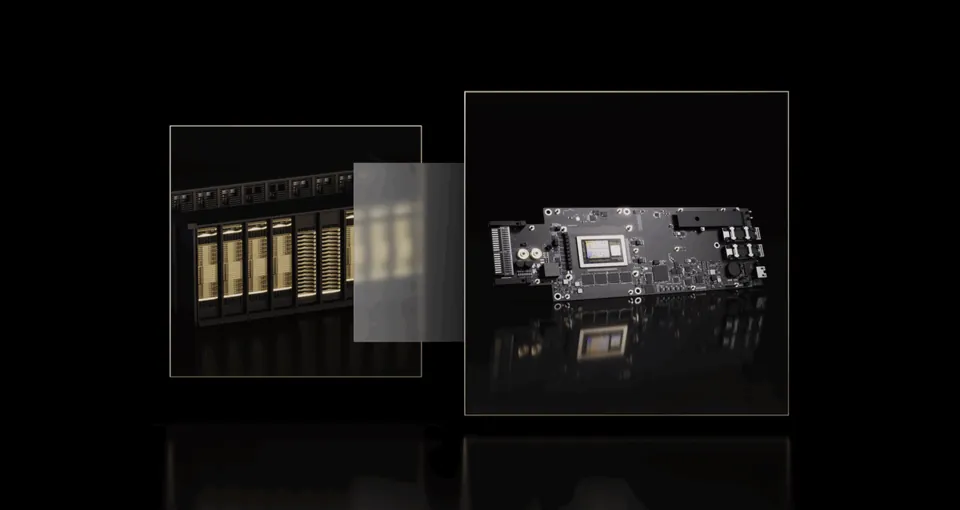
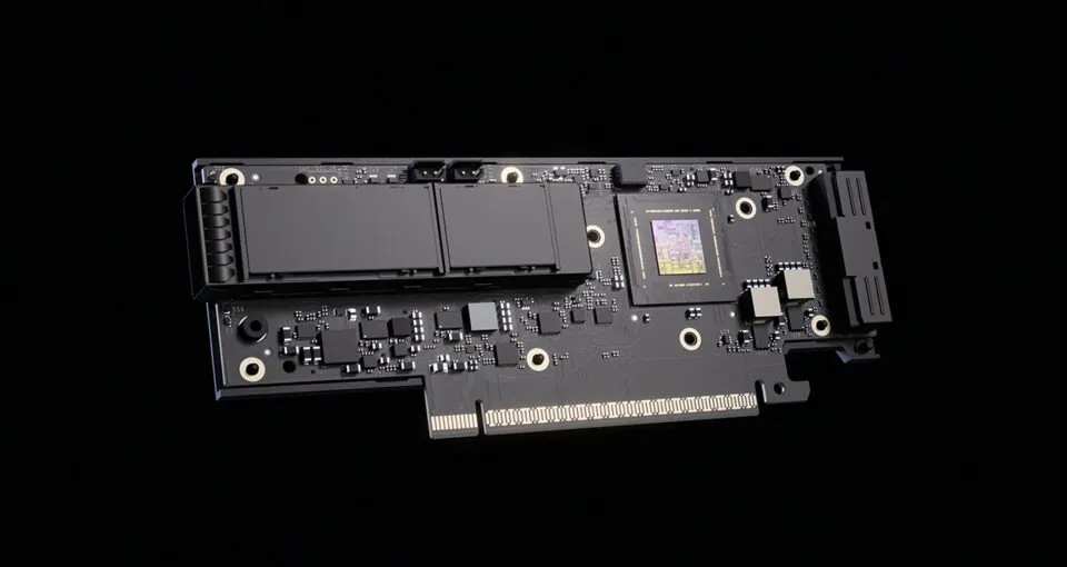
Today, NVIDIA’s dominance is less about individual components and more about its meticulously crafted, full-stack ecosystem. This integrated approach spans cutting-edge hardware, foundational software, and high-bandwidth interconnects. At the heart of their current offerings are the Hopper (H100/H200) and the newer Blackwell (GB200/GB300) architectures. These GPUs represent monumental leaps in performance, particularly for AI and High-Performance Computing (HPC). Hopper introduced fourth-generation Tensor Cores, dramatically accelerating all precisions including FP8, FP16, and TF32, and delivered up to 30X faster inference for large language models. The H100, for instance, boasts 80GB of HBM3 memory, achieving 3.35 TB/s of bandwidth. Blackwell further refines this with the B200 and the upcoming B300 (Blackwell Ultra) GPUs, featuring up to 192GB HBM3E memory with 8 TB/s bandwidth, and projected FP4 performance of 10-15 PFLOPS per package. This raw power is orchestrated by CUDA, NVIDIA’s ubiquitous software platform, which provides developers with a robust environment for parallel programming. Complementing this, NVLink and NVSwitch technologies create a cohesive, high-bandwidth fabric, allowing GPUs to communicate at speeds far beyond traditional PCIe, effectively forming a single, massive accelerator for the most demanding workloads.
The Interconnect Backbone: NVLink, NVSwitch, and DPUs
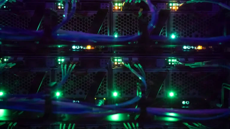
Scaling AI and HPC workloads requires not just powerful GPUs, but an equally sophisticated network backbone. NVIDIA addresses this with its advanced interconnect technologies: NVLink, NVSwitch, and the groundbreaking NVL72 architecture. NVLink provides high-bandwidth, low-latency communication directly between GPUs and between GPUs and CPUs (as seen in Grace Hopper and Grace Blackwell Superchips), facilitating efficient data exchange within a node. NVSwitch then extends this connectivity, enabling multiple GPUs to form large, unified memory domains across servers, with the NVL72 design allowing 72 GPUs to operate as a single, massive accelerator in a rack. NVIDIA’s foresight in recognizing the criticality of networking led to the strategic acquisition of Mellanox, a move Jensen Huang considers one of his best. This acquisition has been pivotal in developing advanced networking solutions like the BlueField Data Processing Units (DPUs) and Quantum-X Photonics InfiniBand. BlueField DPUs offload, accelerate, and isolate data center functions such as networking, storage, and security, freeing up GPUs and CPUs for compute-intensive tasks. Coupled with Quantum-X Photonics CPO (Co-Packaged Optics) networking switches, these technologies are integral to building the ‘AI factories’ and exascale supercomputers of the future, drastically reducing energy consumption and operational costs while ensuring unprecedented scalability and resiliency.
The AI Tsunami: Scaling Intelligence with GPUs
The current explosion of AI, particularly in large language models (LLMs), generative AI, agentic AI, and physical AI, is fundamentally powered by the unique capabilities of GPUs. Their parallel processing architecture makes them perfectly suited for the massive matrix multiplications and tensor operations that define AI training and inference. As Jensen Huang articulates, the world is now producing ‘tokens’ — floating-point numbers that represent intelligence — at an extraordinary scale, turning data centers into ‘AI factories.’ This phenomenon is driven by scaling laws, which demonstrate that larger models, trained on larger datasets, with more compute, yield exponentially better results. This continuous demand for more powerful GPUs and integrated systems is creating an economic engine measured in trillions of dollars, necessitating massive investments in AI infrastructure. Companies are in a race to build these AI factories, recognizing that the ability to generate and process intelligence at scale will redefine industries and create unprecedented value.
The Road Ahead: NVIDIA’s Future Architectures & Roadmap to 2028
NVIDIA’s ambition is far from sated, as evidenced by its aggressive and transparent roadmap extending through 2028. Following Blackwell, the next-generation GPUs, codenamed Rubin (VR200/VR300), are slated for 2026 and 2027. These will feature significantly enhanced FP4 performance, with the VR300 (Rubin Ultra) projected to reach 100 PFLOPS per package. Memory advancements are equally striking, moving to HBM4 and HBM4E, with the VR300 boasting a colossal 1 TB of HBM4E memory and 32 TB/s of bandwidth, demanding up to 3600W TDP. Accompanying these GPUs will be the Vera CPUs, packing 88 custom Arm cores. Looking further, the Feynman generation of GPUs is anticipated for 2028, promising even greater computational density. The interconnect landscape will also evolve, with NVLink 6.0 and 7.0 increasing bandwidth to 3.6 TB/s and beyond. Networking will see the introduction of Spectrum 7 Ethernet and CX10 InfiniBand optical interconnects, pushing speeds to 3.2 Tb/s per port, ensuring that NVIDIA’s full-stack approach continues to deliver unparalleled scalability for the AI era.
NVIDIA Enterprise GPU Roadmap (2022-2028)
| Architecture | Year | GPU | FP4 PFLOPs | Memory | Bandwidth | TDP | CPU |
|---|---|---|---|---|---|---|---|
| Hopper | 2022 | H100 | N/A | 80 GB HBM3 | 3.35 TB/s | 700 W | N/A |
| Hopper | 2023 | H200 | N/A | 141 GB HBM3E | 8 TB/s | 700 W | N/A |
| Blackwell | 2024 | B200 | 10 | 192 GB HBM3E | 8 TB/s | 1200 W | 72-core Grace |
| Blackwell Ultra | 2025 | B300 | 15 | 288 GB HBM3E | 4 TB/s | 1400 W | 72-core Grace |
| Rubin | 2026 | VR200 | 50 | 288 GB HBM4 | 13 TB/s | 1800 W | 88-core Vera |
| Rubin Ultra | 2027 | VR300 | 100 | 1 TB HBM4E | 32 TB/s | 3600 W | 88-core Vera |
| Feynman | 2028 | Feynman | TBD | Next-gen HBM | TBD | TBD | 88-core Vera |
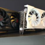
The Competitive Landscape: AMD’s Instinct MI300 Series
While NVIDIA commands a dominant position, the competitive landscape is not static. AMD has emerged as a formidable challenger, particularly with its Instinct MI300 series accelerators. Based on the CDNA 3 architecture, the MI300 series is designed to tackle demanding AI and HPC workloads. AMD’s strategy emphasizes heterogeneous integration, offering both MI300A (an APU that combines ‘Zen 4’ x86 CPUs with CDNA 3 GPU chiplets) and the MI300X (a GPU-only accelerator). The MI300X, for example, features up to 192GB of HBM3 memory and a theoretical peak memory bandwidth of 5.3 TB/s, offering competitive FP8 and FP16 performance. AMD supports these accelerators with its open-source ROCm software platform, aiming to provide a flexible and customizable ecosystem for developers. This approach offers an alternative to NVIDIA’s tightly integrated stack, appealing to organizations that prioritize open standards and vendor diversity.
NVIDIA vs. AMD: Flagship AI/HPC Accelerators
| Feature | NVIDIA H100 SXM5 | NVIDIA B200 | AMD Instinct MI300X |
|---|---|---|---|
| Architecture | Hopper | Blackwell | CDNA 3 |
| Year | 2022 | 2024 | 2023 |
| Memory Capacity | 80GB HBM3e | 192GB HBM3E | 192GB HBM3 |
| Memory Bandwidth | 3.35 TB/s | 8 TB/s | 5.3 TB/s |
| TDP (W) | 700 | 1200 | ~700 |
The Gamer’s Reality Check: Bridging the Gap Between Vision and Experience
Despite the awe-inspiring advancements in high-performance computing, a palpable disconnect exists with the average PC gamer. Our community often views the rapid proliferation of upscaling and frame generation technologies, such as NVIDIA’s DLSS and AMD’s FSR, with a degree of skepticism and frustration. Rather than pure performance gains, these innovations are frequently perceived as ingenious workarounds for what many gamers feel is a lack of fundamental optimization in modern titles. This sentiment is exacerbated by the constant stream of proprietary features that often lock users into specific ecosystems or demand the latest, most expensive hardware, leaving those with older architectures feeling left behind. The sheer volume of confusing acronyms — FSR1/2/3, FSRR, AFMF, DLSS, XeSS, XeLL, XeFG — further contributes to a general weariness, making it challenging for even enthusiastic users to keep pace with the ever-evolving GPU landscape and discern genuine progress from marketing jargon.
Gamers’ Pulse: The Unseen Costs of Progress
While the industry accelerates, PC gamers express deep skepticism, frustration, disappointment, and confusion regarding the rapid, often proprietary, evolution of GPU technologies.
The Philosophical Divide: Full-Stack Control vs. Open Ecosystems
NVIDIA’s enduring strategy centers on building a cohesive, end-to-end platform. This involves meticulous control over every layer: from the hardware (GPUs, Grace CPUs, DPUs) to the foundational software (CUDA, cuDNN, TensorRT). However, this comes with inherent disadvantages, including potential vendor lock-in and higher costs. In contrast, competitors like AMD champion a more open, flexible approach with platforms like ROCm, which aims for broader compatibility. This philosophical divide shapes not just product offerings but the very trajectory of accelerated computing.
NVIDIA’s Full-Stack Strategy
Pros
- Unparalleled Performance & Efficiency via co-design.
- Mature & Robust CUDA Ecosystem.
- Seamless Scalability for exascale AI.
- Rapid Architectural Innovation.
Cons
- High Cost & Entry Barrier.
- Proprietary Lock-in (CUDA).
- Consumer Frustration with rapid hardware cycles.
- Geopolitical Vulnerability (Supply Chain).
Final Verdict: NVIDIA’s Silicon Supremacy
NVIDIA stands at the zenith of a computing paradigm shift, having successfully transitioned from a graphics card company to the architect of accelerated computing. Their relentless pursuit of a full-stack ecosystem has created an almost insurmountable lead in the AI and supercomputing race. While gamer skepticism remains high regarding optimization, NVIDIA’s roadmap through 2028 suggests an unwavering commitment to scaling intelligence that will forever change the digital landscape.