Key Takeaways
- Intel and Nvidia have partnered to create ‘RTX SoCs’—premium integrated chips combining Intel x86 CPUs and Nvidia RTX GPU chiplets.
- The core technological advantage is NVLink, providing up to 900 GB/s on-package bandwidth to challenge AMD’s monolithic APUs (like Strix Halo).
- The partnership is backed by a $5 billion Nvidia investment in Intel, but the first consumer products are not expected until 2027, carrying significant risk.
The Unthinkable Alliance: Why Intel and Nvidia Shook Hands
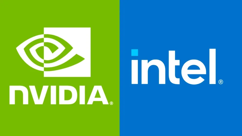
The semiconductor world was stunned by the joint confirmation: Intel and Nvidia, long-time rivals in the graphics space, are officially collaborating on a new class of integrated chips. This multi-generational partnership, sealed by a massive $5 billion investment from Nvidia into Intel, is not just a business deal; it is a strategic maneuver designed to recapture the high-growth markets of premium gaming laptops and consumer AI. For Intel, this massive financial injection provides a much-needed lifeline amid restructuring, linking them directly to the world’s most valuable semiconductor company. For Nvidia, it’s a direct path to integrate their dominant RTX IP—the consumer mindshare leader—into the vast x86 ecosystem, bypassing the need for a discrete GPU in many high-end systems and directly challenging AMD’s integrated dominance.
Deconstructing the RTX SoC: The NVLink Bandwidth Bomb
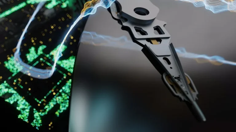
The ‘RTX SoC’ is not a traditional integrated graphics solution; it is a declaration of war built on silicon engineering. It represents a complex multi-die package, fusing Intel x86 CPU tiles with Nvidia RTX GPU chiplets. This asymmetric design requires Intel’s most advanced packaging technologies—Foveros 3D and EMIB—to connect components built on potentially different process nodes and fabs, a massive undertaking in integration complexity. However, the true game-changer, and the reason this collaboration is viable, is the use of Nvidia’s proprietary NVLink interconnect to bind the components. This ‘on-package’ link offers a staggering 900 GB/s of bandwidth, which is more than ten times faster than a standard PCIe 4.0 connection. This high-speed, ultra-low-latency connection is key to enabling efficient unified memory sharing, effectively eliminating the memory bottlenecks that plague current integrated solutions and promising a performance leap that could redefine the power-to-performance ratio of integrated computing.
RTX SoC (Projected) Key Technical Differentiators
- CPU Architecture
- Intel x86 Cores (Tile-based)
- GPU Architecture
- Nvidia RTX GPU Chiplets (TSMC-made)
- Interconnect Technology
- NVLink (Chip-to-Chip)
- Peak Bandwidth
- Up to 900 GB/s
- Packaging
- Intel Foveros 3D / EMIB
- Target Market
- Premium Laptops, Mini-PCs, Consumer AI
The Competitive Arena: AMD’s Strix Halo vs. The Fusion Protocol
The primary target of the RTX SoC is clear: AMD’s highly successful APU line. AMD, particularly with its upcoming Ryzen AI 300 series (codenamed Strix Halo), currently dominates the premium integrated market, holding a decisive lead in gaming handhelds and high-performance notebooks. Strix Halo utilizes a vertically integrated, monolithic die design built on TSMC’s 4nm process, featuring powerful RDNA 3.5 graphics and a dedicated NPU. While AMD’s monolithic approach is cheaper to manufacture and generally easier to bin, the Intel-Nvidia partnership aims to leapfrog this with raw interconnect speed. The core conflict is philosophical: can the complexity of integrating asymmetric chiplets from two different vendors via NVLink truly overcome the manufacturing and cost advantages inherent in AMD’s single, unified die design?
Integrated Chip Architecture Showdown
| Feature | AMD Strix Halo (Current Leader) | Intel-Nvidia RTX SoC (2027 Target) |
|---|---|---|
| GPU Integration | Monolithic (Integrated RDNA 3.5) | Chiplet (Nvidia RTX GPU Tile) |
| Inter-Component Link | Standard On-Die Bus | NVLink (900 GB/s) |
| Memory Sharing | Unified LPDDR5X (High Latency) | Unified Memory (Ultra-Low Latency) |
| Manufacturing Complexity | Low (Single Die, Single Fab) | High (Multi-Die, Multi-Fab) |
History Repeats? The Kaby Lake-G Warning
Enthusiasts are right to be cautious about this unprecedented collaboration. This is not Intel’s first foray into integrating rival graphics onto a single package. The 2017 Kaby Lake-G project, which fused Intel CPUs with AMD Radeon GPUs using EMIB packaging, was a technical marvel that delivered strong performance but failed to survive a single product generation due to complexity, high cost, and lack of long-term commitment from both parties. The extended 2027 timeline for the RTX SoC suggests Intel and Nvidia are prepared for a long haul, backed by a massive investment, but the failure of Kaby Lake-G remains a critical historical precedent that demands rigorous scrutiny.
The Arc Question: What Does This Mean for Intel’s Own GPUs?
Intel has been quick to insist that the Nvidia partnership is ‘complementary’ to their existing roadmap. Officially, the development of Arc discrete graphics (Battlemage and Celestial) and integrated Arc Xe3 iGPUs for future platforms like Panther Lake and Nova Lake continues as planned. However, the long-term viability of Intel’s internal graphics efforts is now an open question, especially given the $5 billion commitment to the RTX SoC. If the Nvidia-infused SoCs prove to be a massive success and capture the premium segment, market pressure and internal strategy could see Nvidia’s dominant IP eventually replace Intel’s own integrated offerings entirely. Some industry sources speculate this transition could happen as early as the Titan Lake platform around 2028. For now, Arc is safe, benefiting from Intel’s renewed focus on gaming, but the clock is ticking on its long-term strategic relevance.
The Consumer Impact: Pros and Cons of the RTX SoC
Pros (Potential Advantages)
- Unprecedented integrated graphics performance thanks to NVLink bandwidth.
- Potential for smaller, more power-efficient high-end laptops (reduced thermal juggling and simpler power subsystems).
- Nvidia’s dominant AI/RTX software stack integrated directly into the CPU platform.
Cons (Potential Drawbacks)
- High complexity could lead to production delays (the 2027 timeline is lengthy and subject to change).
- Potential for significantly higher price points than AMD’s monolithic APUs.
- Long-term threat to Intel’s Arc GPU development, reducing overall market competition and innovation.
Final Verdict: A High-Stakes Gamble
The Intel-Nvidia partnership is the most significant strategic alliance in PC hardware this decade. It’s a desperate, high-stakes attempt by two industry giants to halt AMD’s momentum in the integrated space by leveraging the one thing AMD cannot match: Nvidia’s dominant RTX IP and the staggering bandwidth of the NVLink interconnect. If they can successfully navigate the immense engineering challenges of integrating asymmetric chiplets by the 2027 target, the resulting RTX SoCs could truly redefine what a gaming laptop is capable of, delivering desktop-class performance in a highly efficient form factor. However, the lengthy timeline and the ghost of Kaby Lake-G mean this is a high-risk, high-reward gamble that will test the patience of the entire enthusiast community and the stability of the alliance itself.
Frequently Asked Questions (FAQ)
What is the primary goal of the NVLink connection in the RTX SoC?
The primary goal is to provide ultra-high bandwidth (up to 900 GB/s) and low latency between the Intel CPU tile and the Nvidia GPU chiplet, enabling efficient unified memory sharing that is far superior to standard PCIe connections.
When are the first RTX SoCs expected to launch?
While the partnership is active now, the first consumer products utilizing the RTX SoC are not expected to hit the market until 2027.
Will this partnership affect Intel’s data center business?
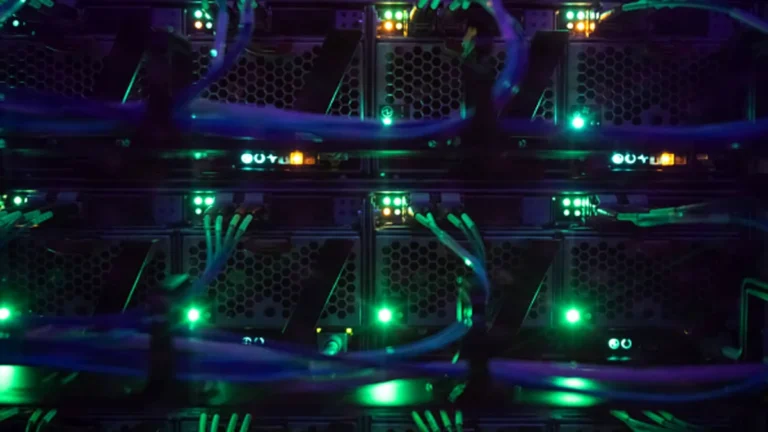
Yes. The collaboration also covers the data center, where Intel will design and manufacture custom x86 CPUs optimized for Nvidia’s AI infrastructure, integrated via NVLink interconnects, establishing Intel as Nvidia’s premier x86 partner.