Key Takeaways
- The B850 chipset frequently represents an ‘X870 killer’ in disguise, mandating PCIe 5.0 for NVMe and offering VRM architectures—like the 12+2+1 60A SPS system on the MSI B850MPOWER—that rival flagship-tier engineering.
- For extreme memory overclocking, 2-DIMM boards are the superior choice. The B850MPOWER’s specialized trace layout facilitates speeds up to 10,200 MT/s, challenging the necessity of the X870 luxury chipset tax for performance seekers.
- Pricing resentment is justified at the $300 tier; boards like the ASUS ROG Strix B850-G offer robust 80A power stages but inexplicably omit alphanumeric debug LEDs, a critical diagnostic tool at this price point.
- Platform stability is contingent on the 1.2V SoC voltage cap mandated by recent AGESA updates. This safety measure is non-negotiable for Zen 5 longevity, though it necessitates precision tuning for Infinity Fabric (FCLK) stability beyond 2200MHz.
- The Promontory 21 die is shared across B850 and X870; the primary differentiators are mandatory USB4 and PCIe 5.0 graphics lanes on X870, features that many mainstream builders may find redundant given the 4-lane CPU-to-chipset bottleneck.
The Stability Imperative: Addressing the AM5 Voltage Crisis
The recent launch of the B850 series, tailored for the new Ryzen 9000 (Zen 5) mainstream segment, represents a major architectural win for builders seeking value. However, any discussion of new AM5 hardware must begin with the elephant in the socket: the lingering instability issues that have plagued the platform since its inception. Following widespread reports of CPU failures, AMD confirmed that the root cause was improper BIOS configuration, which inadvertently pushed critical processor voltages beyond safe operating limits. This crisis necessitated a platform-wide, immediate response from every major motherboard vendor. For any builder—especially those integrating a new B850 board into a high-performance Zen 5 system—understanding and applying these stability fixes is not optional; it is a mandatory engineering protocol.
To mitigate hardware degradation, vendors have enforced a 1.2V cap on the System-on-a-Chip (SoC) voltage (VDDCR_SOC). While this is vital for CPU safety, it introduces a hard ceiling for low-level tuning. Specifically, Zen 5’s Infinity Fabric (FCLK) stability is highly sensitive to SoC voltage. Pushing FCLK toward the 2200MHz (4400MHz effective) threshold or utilizing high-speed DDR5 kits (8000MT/s+) within this 1.2V envelope requires meticulous sub-timing optimization. Builders must understand that while 1.2V is the ‘safe’ harbor, it tightens the margin for error in memory latency tuning. Ensure your BIOS is updated to the latest AGESA standard to lock these safety parameters before attempting any EXPO or manual frequency scaling.
Engineering Deconstructed: B850 vs. X870 Chipset Mandates
| Feature | X870E (Premium) | X870 (High-End) | B850 (Mid-Range) | B840 (Entry-Level) |
|---|---|---|---|---|
| CPU Overclocking | Advanced (Required) | Advanced (Supported) | Moderate (Supported) | Disabled |
| PCIe 5.0 GPU Support | Mandatory (x16 or x8/x8) | Mandatory (x16 or x8/x8) | Optional (Typically Gen 4) | Disabled (Max Gen 3) |
| PCIe 5.0 NVMe Support | Mandatory (At least 1 slot) | Mandatory (At least 1 slot) | Mandatory (At least 1 slot) | Disabled (Max Gen 3) |
| Mandatory USB Standard | USB4 (40 Gbps) | USB4 (40 Gbps) | USB 3.2 Gen 2×2 (20 Gbps) | USB 3.2 Gen 2 (10 Gbps) |
| Chipset Die | Dual Promontory 21 | Single Promontory 21 | Single Promontory 21 | Promontory 19 (Older) |
The B850 chipset is built on the same modern silicon—the Promontory 21 die—as the higher-end X870 series. This shared silicon heritage is significant; the X870 simply utilizes a more expansive implementation, often incorporating discrete controllers like the Asmedia ASM4242 to provide mandatory USB4 (40 Gbps) and DisplayPort Alt Mode. While B850 mandates PCIe 5.0 for the primary NVMe slot, it leaves Gen 5 support for the GPU as an optional feature for vendors to differentiate their product stacks.
However, a critical engineering bottleneck remains: the 4-lane CPU-to-chipset uplink. Regardless of whether you use a single or dual Promontory 21 configuration, all chipset-bound I/O—including secondary M.2 slots, SATA controllers, and 5GbE LAN—must compete for bandwidth across this narrow channel. This architectural reality often makes the ‘Extreme’ designations more about connectivity quantity than raw throughput quality, reinforcing the value proposition of high-end B850 boards that prioritize direct-to-CPU lanes for primary performance components.
Hardware Engineering Deconstructed: B850 VRM & PCB Forensics
To separate marketing hyperbole from engineering reality, we must look at the component level. A true forensic analysis of a motherboard requires scrutinizing the PWM controller and MOSFET selection—the silicon that actually keeps your Ryzen 9 9950X from throttling. By performing a teardown of the VRM and analyzing the PCB’s thermal characteristics, we can identify ‘sleeper’ B850 boards that provide flagship-level power delivery at a mid-range price point, effectively bypassing the luxury chipset tax.
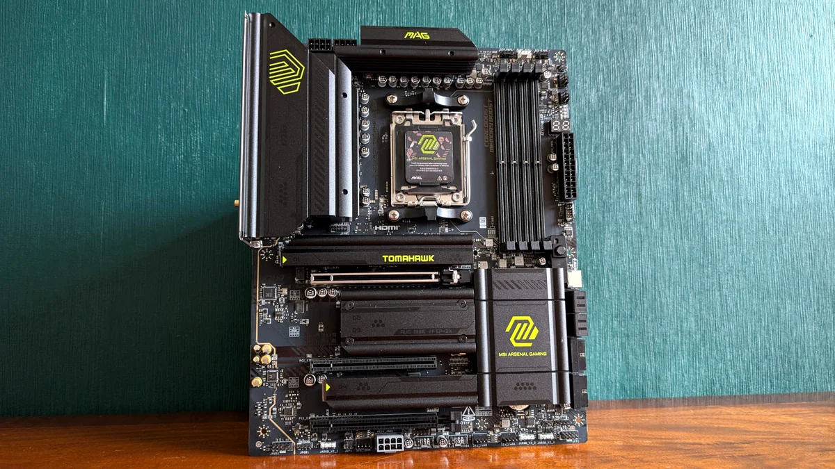
MSI B850MPOWER: A 2-DIMM Overclocking Powerhouse
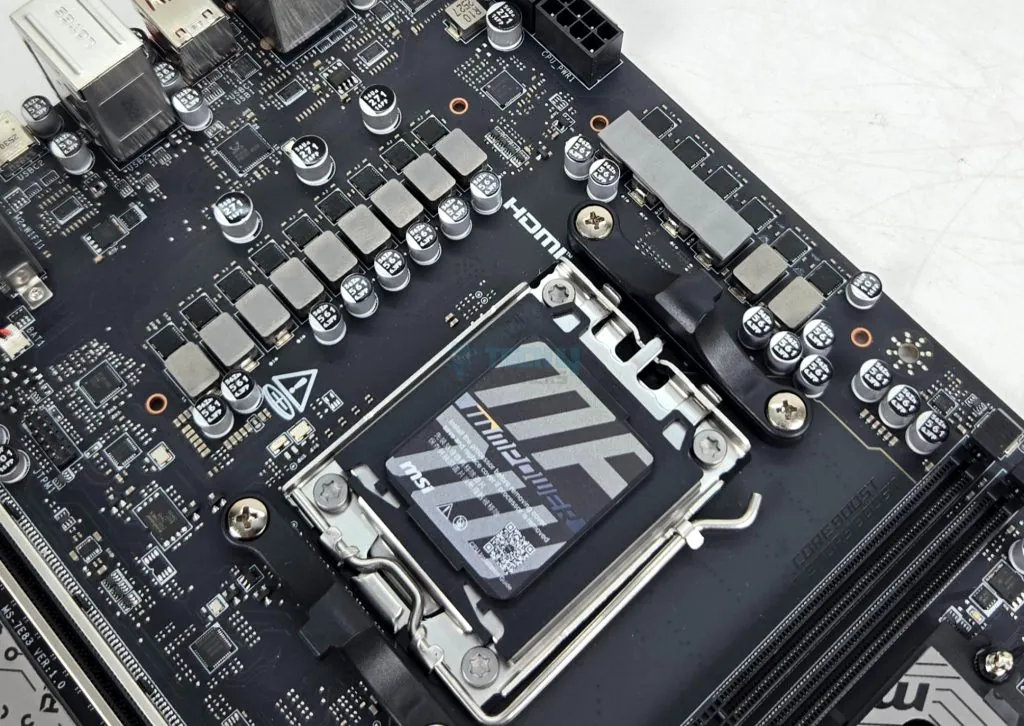
The MSI B850MPOWER is a masterclass in focused engineering. Its VRM utilizes a 12+2+1 Duet Rail Power System driven by the MPS2309/MP2857 PWM controller, with 14 phases managed by MPS2519/MP8766 power stages. The VCore phases utilize 60A Smart Power Stages (SPS), which, when paired with an 8-layer server-grade PCB and 2oz thickened copper, results in exceptional thermal efficiency. Under a 243W PBO load, we observed MOSFET temperatures peaking at a mere 57°C.
Beyond power delivery, the B850MPOWER is a memory overclocker’s dream. By opting for a 2-DIMM design, MSI has minimized signal interference and trace length, enabling DDR5 frequencies up to 10,200 MT/s (OC). This board also features a dedicated OC Engine—an RC26008 external clock generator—allowing for independent BCLK adjustments. This level of granular control is usually reserved for $500+ flagship boards, making this mATX offering a formidable performance vanguard.
ASUS ROG Strix B850-G Gaming WiFi: Premium, But With a Glaring Omission
The ASUS ROG Strix B850-G Gaming WiFi represents the premium tier of the B850 ecosystem, featuring a heavy-duty 14+2+1 power solution with 80A stages. This is overkill for almost any current AM5 processor, providing massive headroom for stability. The inclusion of PCIe Slot Q-Release and M.2 Q-Latch shows a commitment to DIY quality of life. However, at a price point nearing $300, the absence of a dedicated alphanumeric debug LED display is a significant engineering regression. While the Q-LED system provides basic status checks, the lack of precise POST codes on a board of this caliber is a point of valid pricing resentment for enthusiasts who demand professional-grade troubleshooting tools.
The mATX Vanguard: Flagship B850 Boards Analyzed
| Feature | MSI B850MPOWER (mATX OC Focus) | ASUS ROG Strix B850-G Gaming WiFi (mATX Premium) |
|---|---|---|
| Form Factor | Micro-ATX (243.84×243.84mm) | Micro-ATX (244x244mm) |
| VRM Power Stages | 12+2+1 Duet Rail (60A SPS) | 14+2+1 (80A per stage) |
| PWM / MOSFETs | MPS2309/MP2857 / MPS2519/MP8766 | ASUS DIGI+ VRM / 80A Power Stages |
| PCB Layers | 8-Layer Server Grade (2oz Copper) | 8-Layer |
| DIMM Slots / OC | 2x DIMM / 8400+ MT/s (OC) | 4x DIMM / 8000+ MT/s (OC) |
| PCIe 5.0 x16 Slot | Yes (Steel Armor) | Yes (SafeSlot) |
| M.2 Slots (5.0/4.0) | 4 Total (2x Gen 5, 2x Gen 4) | 4 Total (1x Gen 5, 3x Gen 4) |
| Unique Feature | OC Engine (BCLK Gen) / 2-DIMM Design | Q-Release & Q-Latch / NO Debug LED |
Engineering Architecture Highlights:
- Dual 8-Pin EPS Connectors for high-wattage Zen 5 stability
- 12+2+1 Duet Rail VRM with 60A Smart Power Stages
- MPS2309/MP2857 PWM Controller handling VCore/SoC logic
- 8-Layer Server-Grade PCB with 2oz Thickened Copper
- Optimized 2-DIMM Memory Slots for 10,200 MT/s+ signaling
- RC26008 OC Engine for external BCLK generation
- EZ Dashboard header for physical Power/Reset/Debug connectivity
The mATX Compromise: Cooling and Clearance
Pros
- Smaller Footprint: Ideal for compact, powerful builds (e.g., Lian Li A3-mATX).
- Cost Efficiency: Often cheaper than equivalent ATX boards while retaining most features.
- High Feature Density: Flagship mATX boards now offer 4+ M.2 slots and Gen 5 support.
Cons
- GPU Clearance: Large RTX/Radeon cards can block access to lower headers and M.2 slots.
- Thermal Challenge: Reduced heatsink mass and less overall airflow space compared to full ATX.
- Limited Expansion: Usually only one usable PCIe x16 slot, restricting multi-card setups.
The Price Paradox: When B850 Meets X870
“I came very close to getting the B850 Tomahawk Max, but it was so close in price to the X870 Tomahawk, that it was a no-brainer to go for the X870. It has a couple improvements of which the most notable are much better cooling for the primary gen 5 SSD slot and a debug LED display.”
— LoadSyn Community Member Quote (Fandom Pulse)
VRM Thermal Performance: High-End B850 vs. X870 (Full Load)
Measured in Degrees Celsius (°C) – Lower is Better
The most acute point of ‘Pricing Resentment’ in current motherboard stacks is the omission of alphanumeric debug LEDs on boards like the ASUS ROG Strix B850-G or B850-F. When builders pay a premium—often $300 or more—they expect professional-grade diagnostic tools. Relying on four simple Q-LEDs for a ‘premium’ board is a cost-cutting measure that creates significant ‘Value Anxiety.’ If you are troubleshooting a complex memory training issue or an FCLK instability, the difference between a generic ‘DRAM’ light and a specific ‘Code 15’ is the difference between an hour of frustration and five minutes of progress.
Final Verdict
The B850 chipset has successfully challenged the hegemony of the ‘Extreme’ chipsets by delivering flagship-tier engineering where it counts: power delivery and storage speed. For the performance-empowered gamer, a board like the MSI B850MPOWER provides the 2-DIMM signal integrity and 60A SPS power stages necessary to push Zen 5 to its limits without the X870 tax. However, the ‘Price Paradox’ is real. If you demand the quality-of-life convenience of an alphanumeric debug LED or the guaranteed bandwidth of USB4, the X870 remains the undisputed choice. For everyone else, the B850—provided you maintain a strict 1.2V SoC voltage limit and update your BIOS—is the definitive engineering sweet spot for the AM5 platform.
Frequently Asked Questions
Will my Ryzen 9000 (Zen 5) CPU work on my existing 600-series AM5 motherboard?
Yes, AMD has committed to AM5 longevity. Ryzen 9000 CPUs are compatible with existing X670 and B650 boards, though a critical BIOS update will be necessary for full stability, optimized clock speeds, and complete feature support.
What if my CPU failure was caused by a defective memory controller, not voltage?
Persistent DRAM errors (often indicated by Q-Code 07 or a solid DRAM LED) that remain after swapping both the memory modules and the motherboard strongly suggest a defective integrated memory controller (IMC) on the CPU itself. This is a CPU fault, not a motherboard fault, and requires an AMD RMA.
Is the B840 chipset worth considering for budget builds?
The B840 is highly constrained, being restricted to PCIe 3.0 speeds for chipset-connected lanes and lacking CPU overclocking support. It is only suitable for entry-level, energy-efficient systems using Ryzen G-Series processors.
How does the 1.2V SoC voltage limit impact FCLK stability and memory latency on Zen 5?
The 1.2V SoC voltage cap is an engineering trade-off for safety. While it prevents silicon degradation, it limits the electrical headroom for the memory controller. This creates a ceiling for Infinity Fabric (FCLK) stability, often making it difficult to push past 2200MHz without encountering WHEA errors. Consequently, achieving ultra-low memory latency at DDR5-8000+ speeds becomes a matter of meticulous sub-timing tuning. Boards with 2-DIMM designs, like the MSI B850MPOWER, offer a significant advantage here by providing cleaner signal paths, which allows for higher stable frequencies even at the lower 1.2V SoC limit.