Key Takeaways
- SMIC’s N+3 process, confirmed in Huawei’s Kirin 9030, marks China’s significant step towards 5nm-class chip manufacturing without EUV technology.
- This advancement relies on Deep Ultraviolet (DUV) lithography combined with complex multi-patterning techniques (SAQP), a ‘brute-force’ method with inherent challenges.
- While impressive, SMIC’s N+3 still lags behind leading 5nm nodes from TSMC and Samsung in density and efficiency, highlighting the yield and cost trade-offs of DUV-only scaling.
- The global semiconductor race is shifting beyond mere miniaturization, with advanced packaging, chiplets, and new materials becoming crucial battlegrounds.
- China’s aggressive state-backed drive for semiconductor self-sufficiency, fueled by massive subsidies and talent acquisition, continues to reshape the industry amidst geopolitical tensions.
Introduction: The New Semiconductor Frontier
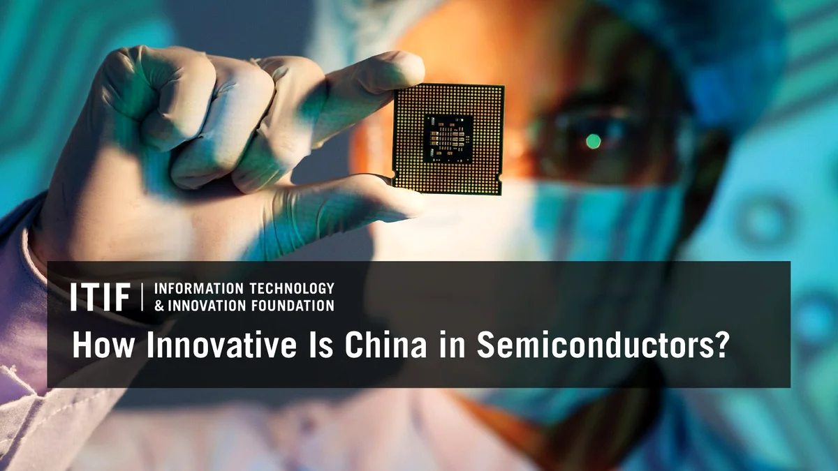
The semiconductor industry is a relentless arena of innovation, where every nanometer counts in the race for performance and efficiency. For years, the narrative has been dominated by industry titans like TSMC, Samsung, and Intel, pushing the boundaries with cutting-edge Extreme Ultraviolet (EUV) lithography. But a new player has made an undeniable statement: China’s Semiconductor Manufacturing International Corporation (SMIC). With the recent launch of Huawei’s Mate 80 series, powered by the Kirin 9030 processor, TechInsights’ teardowns have confirmed the use of SMIC’s N+3 process – an impressive leap that signals China’s determined march towards 5nm-class manufacturing, all without access to the most advanced EUV tools. This achievement not only redefines the competitive landscape but carries profound implications for the future of global tech, including the gaming hardware that powers our digital worlds.
Deconstructing the Kirin 9030: SMIC’s N+3 Process Unveiled
The heart of Huawei’s latest flagship, the Kirin 9030, has been the subject of intense industry speculation. Was it 5nm? An enhanced 7nm? The definitive answer, provided by detailed analysis from TechInsights, confirms its manufacturing on SMIC’s N+3 process. This isn’t a direct 5nm node in the same vein as TSMC or Samsung’s offerings, but rather a ‘scaled evolution of its 7nm-class technology.’ Crucially, it represents a significant advancement for SMIC, pushing the boundaries of what’s possible with Deep Ultraviolet (DUV) lithography. While SMIC itself hasn’t officially detailed its N+3 roadmap, the Kirin 9030 serves as a tangible, real-world validation of China’s progress, showcasing meaningful density improvements that bring it closer to a true 5nm-equivalent node. This achievement, under the shadow of stringent US sanctions, highlights a remarkable resilience and an innovative approach to overcoming technological barriers.
Key Semiconductor Process Node Comparisons
| Process Node | Manufacturer | Lithography Tech | Transistor Density (approx. MTr/mm²) | Status / Key Use |
|---|---|---|---|---|
| N+3 | SMIC | DUV (Multi-patterning) | 130 (expected) | Kirin 9030 (Mate 80 series) |
| 7nm (N+2) | SMIC | DUV (Multi-patterning) | ~90-100 | Kirin 9000S (Mate 60 Pro), AI Accelerators |
| 5nm (N5) | TSMC | EUV | ~134-173 | iPhone 12/13/14, M1/M2 chips |
| 4nm (N4) | TSMC | EUV | ~140-180 | iPhone 15 Pro, Snapdragon 8 Gen 2 |
| 3nm (N3E) | TSMC | EUV | ~200-250 | iPhone 15 Pro Max, M3/A17 Pro chips |
| 2nm (N2) | TSMC | GAAFET (EUV) | ~250-300 (est) | Mass production Q4 2025 |
| 2nm (SF2) | Samsung | GAAFET (EUV) | ~200-240 (est) | Exynos 2600 (mass production Q4 2025) |
The DUV Dilemma: Multi-Patterning as a Necessity
The primary hurdle for SMIC’s advanced node development is the lack of access to Extreme Ultraviolet (EUV) lithography machines, critical tools for etching the infinitesimally small circuits required for 5nm and beyond. Due to export controls, SMIC is forced to rely on older, Deep Ultraviolet (DUV) lithography. To achieve higher transistor densities with DUV, manufacturers employ a ‘brute-force’ technique called multi-patterning, specifically self-aligned quadruple patterning (SAQP) for advanced nodes like 5nm and even 3nm-class. This method involves repeatedly etching lines on silicon wafers multiple times to boost transistor density. While technically feasible, DUV multi-patterning is notoriously complex, leading to significantly increased manufacturing steps, longer production times, higher costs, and often lower yields compared to the more efficient single-pass EUV process. Intel, for example, faced significant delays and complications when attempting to use SAQP for its initial 10nm nodes before eventually transitioning to EUV.

The Global Gauntlet: SMIC vs. TSMC, Samsung, and Intel
Leading-Edge Foundry Race: A Snapshot
| Foundry | Most Advanced Node | Lithography Strategy | Key Customers/Products | Yield & Cost Considerations |
|---|---|---|---|---|
| TSMC | 3nm (N3E), 2nm (N2) | EUV (GAAFET for 2nm) | Apple, Qualcomm, NVIDIA, AMD | High yields, optimized cost structure, premium pricing |
| Samsung Foundry | 2nm (SF2) | EUV (GAAFET) | Qualcomm (partially), Exynos | Aggressive tech lead, historical yield challenges, competitive pricing |
| Intel Foundry | Intel 18A (2nm eq) | EUV (RibbonFET/PowerVia) | Internal, external (Expanding) | Catch-up strategy, heavy investment, aiming for mass production |
| SMIC | N+3 (5nm-class) | DUV (multi-patterning) | Huawei (Kirin), domestic AI chips | Lower yields, higher cost per chip, independence focus |
The global race for semiconductor supremacy is accelerating, with TSMC, Samsung, and Intel all pushing towards 2nm and even 1.4nm nodes, largely enabled by advanced EUV technology and innovative transistor architectures like Gate-All-Around (GAAFET). TSMC’s 2nm (N2) is expected to mass produce in Q4 2025, with Samsung’s Exynos 2600 already in mass production on its 2nm process. Intel is making strides with its 18A process (comparable to 2nm), aiming to launch its Panther Lake processors soon. These companies are not just miniaturizing; they are integrating advanced design-technology co-optimization (DTCO) and sophisticated back-end-of-line (BEOL) processes to maximize performance and power efficiency. SMIC’s N+3, while a monumental achievement under sanctions, remains ‘substantially less scaled than industry 5-nanometre processes,’ as TechInsights noted. The debate extends to cost, with TSMC’s 2nm wafers projected to exceed $30,000, almost double that of 4nm, indicating the immense R&D and manufacturing expenses involved. This stark contrast highlights the challenges SMIC faces in competing on density, yield, and cost against EUV-equipped rivals.
Beyond Miniaturization: The Era of Multi-Dimensional Innovation
As the physical limits of silicon miniaturization approach, the semiconductor industry is increasingly shifting its focus to ‘multi-dimensional innovation.’ This involves breakthroughs in materials, architectures, and packaging technologies that allow for greater performance, integration, and power efficiency without solely relying on smaller process nodes.
- Chiplet Technology: Integrating multiple smaller chip dies (chiplets) with different functions and processes into a single package, enabling customized solutions and cost reduction.
- 3D IC Packaging: Vertically stacking chip dies to significantly shorten interconnection distances, improving data transmission speed and integration density.
- CoWoS (Chip-on-Wafer-on-Substrate): An advanced packaging solution for high-performance chips, integrating logic dies, high-speed interconnects, and high-bandwidth memory (HBM).
- New Materials: Exploration of third-generation semiconductors (SiC, GaN) for high-power/high-frequency, and 2D materials (graphene) for extreme miniaturization.
- Design-Technology Co-Optimization (DTCO): Holistic approach to optimize chip design and manufacturing processes concurrently for maximum gains.
Geopolitical Undercurrents: China’s Quest for Autonomy
China’s push for semiconductor independence is not merely economic; it’s a deeply strategic imperative driven by a desire for self-sufficiency and national security, especially in the face of escalating US export controls. Beijing has poured hundreds of billions of dollars into its semiconductor industry through initiatives like the ‘National IC Strategy’ and the ‘Big Fund,’ aiming to establish a fully ‘closed-loop’ domestic ecosystem. This massive state subsidization, which has seen some Chinese firms receive over 40% of their revenues from government support, aims to reduce reliance on foreign technology and cultivate globally competitive enterprises. While US sanctions have undeniably created hurdles, compelling China to innovate with existing DUV equipment, they have also, paradoxically, intensified China’s resolve. The goal is to develop ‘good enough’ domestic technologies to service critical sectors, from telecommunications and electric vehicles to AI and potentially military applications, even if it means higher costs and slower progress than international rivals.
“Put simply, [the] Kirin 9000S is a better designed chip than the West realizes. It has solid power and performance. Even with the lackluster export controls, this is a leading edge chip that would be near the front of the pack in 2021, yet was done with no access to EUV, no access to cutting edge US IP, and intentionally hampered. We cannot overstate how scary this is.” — Dylan Patel, SemiAnalysis
The Fandom’s Pulse: What the Community Thinks
The LoadSyn community, ever attuned to the cutting edge, views China’s relentless pursuit of semiconductor independence with a complex mix of admiration, skepticism, and pragmatic hope. There’s a grudging respect for the focused, state-driven approach that seemingly cuts through bureaucratic delays to achieve ambitious technological milestones, exemplified by the whispers of domestic EUV development. This often leads to cynical comparisons with other nations’ political priorities, perceived as hindering similar high-stakes technological competition. While many recognize the immense technical chasm between a prototype and production-ready advanced lithography, a residual hope persists that this increased competition will ultimately benefit consumers through lower prices and accelerated innovation. Yet, a palpable frustration also exists, particularly regarding the foundational manufacturing capabilities of lagging nations, sparking aspirations for aggressive reverse-engineering or strategic technological leaps to bridge the gap. For our readers, this isn’t just about geopolitics; it’s about the silicon that will power their next-gen gaming experiences, and the strategic plays that will shape its cost and availability.
DUV-Only Advanced Node Strategy: Pros & Cons
Pros
- Technological Autonomy: Reduces reliance on foreign technology and suppliers.
- Innovation Under Constraint: Fosters unique engineering solutions and pushes limits.
- Strategic Leverage: Demonstrates capability despite international sanctions.
- Ecosystem Growth: Stimulates domestic growth across the supply chain.
Cons
- Higher Cost Per Chip: Multi-patterning significantly increases manufacturing steps.
- Lower Yields: Increased complexity results in higher defect rates.
- Slower Production: Multi-step DUV process extends manufacturing time.
- Efficiency Gap: Lags behind EUV in transistor density and power.
- Scalability: Difficult to achieve mass-market cost competitiveness.
Frequently Asked Questions
What is a ‘process node’ (e.g., 7nm, 5nm)?
A process node refers to the manufacturing technology used to create integrated circuits. Historically, the number represented physical dimension, but today it’s primarily a marketing term indicating a generation of technology with a certain level of transistor density and efficiency.
What’s the difference between DUV and EUV lithography?
DUV uses 193nm wavelengths, while EUV uses 13.5nm. EUV allows for finer patterns in a single pass, whereas DUV requires complex ‘multi-patterning’ to reach high densities, increasing cost and complexity.
How does SMIC achieve 5nm-class production without EUV?
SMIC uses self-aligned quadruple patterning (SAQP) with DUV. This involves multiple passes of DUV light to create patterns that would typically require a single EUV exposure.
What are ‘chiplets’ and ‘advanced packaging’?
Chiplets are specialized functional units manufactured separately and integrated into one package. Advanced packaging (like 3D IC) allows these units to be stacked closely, boosting performance beyond monolithic design limits.
How will this impact future gaming hardware and prices?
Increased competition might drive innovation and lower long-term prices, but the high cost of DUV scaling might limit these chips to specific markets initially. Geopolitical factors will continue to influence availability.
China’s Silicon Gambit: A Path Forged in DUV
SMIC’s N+3 process, as showcased in Huawei’s Kirin 9030, represents a significant and undeniable leap for China’s semiconductor industry. Achieving 5nm-class density using DUV multi-patterning is a testament to extraordinary engineering ingenuity and national resolve in the face of severe restrictions. While this ‘brute-force’ approach carries inherent trade-offs in terms of cost, yield, and ultimate efficiency compared to the EUV-driven advancements of TSMC, Samsung, and Intel, it firmly establishes China as a formidable, if uniquely challenged, player in the advanced node arena. For the gaming tech world, this means a more diverse, albeit complex, supply chain in the long run. The future of silicon is not just about smaller numbers; it’s about multi-dimensional innovation, strategic autonomy, and the relentless pursuit of performance, no matter the pathway.