🔑 Key Takeaways: The 18A Advantage
- Intel’s 18A node (2nm-class) is currently ahead of TSMC’s N2 in raw performance metrics, largely due to its architectural innovations (TechInsights score of 2.53 vs. N2’s 2.27).
- 18A introduces two critical technologies: RibbonFET (GAA transistor) and PowerVia (Backside Power Delivery), which separate power and signal routing for greater density and efficiency.
- While Intel claims a performance lead, TSMC’s N2 is projected to achieve higher high-density transistor count (313 MTr/mm²), potentially leading to smaller, cheaper chips.
- The success of 18A is critical for Intel Foundry Services (IFS) to break TSMC’s perceived monopoly and ensure supply chain diversification for major customers.
The New Arms Race: Why 18A is Intel’s Most Critical Node in a Decade
For years, TSMC has held an undeniable lead in advanced silicon manufacturing, driving up costs and creating a virtual monopoly in the 3nm and 2nm space. Intel’s aggressive ‘5 Nodes in 4 Years’ roadmap culminates with the 18A node, a make-or-break moment designed not just to catch up, but to leapfrog their rival. This node is the foundation for future gaming CPUs like Panther Lake and server chips like Clearwater Forest, but its true strategic value lies in attracting external foundry customers to Intel Foundry Services (IFS). The successful execution of 18A is the proof point Intel needs to re-establish itself as a manufacturing powerhouse and fundamentally shift the balance of power in the semiconductor industry.
“The community expresses a strong desire for Intel’s 18A success primarily as a necessary tool to break TSMC’s perceived monopoly and reduce the rising cost of advanced silicon. ‘Need more competition in the 2nm or even 3nm nodes. TSMC currently has a monopoly in this segment having stomped out SMIC, Samsung, Go Flo, and SK Hynix as well as a bunch of other companies.’”
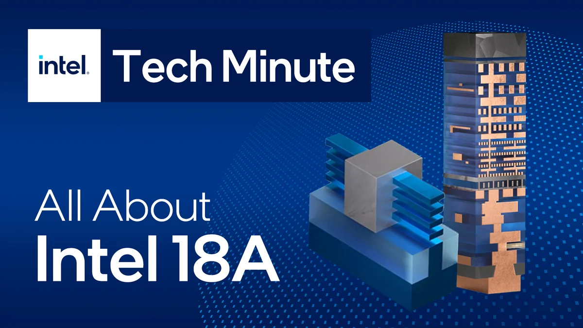
Deconstructed: The Core Technology Behind Intel 18A
Intel 18A vs. TSMC N2: Architectural Feature Showdown
| Feature | Intel 18A (2025 HVM) | TSMC N2 (2025 HVM) |
|---|---|---|
| Transistor Architecture | RibbonFET (GAA) | Nanosheet (GAA) |
| Power Delivery | PowerVia (Backside Power) | Traditional Frontside Power |
| Performance Claim (vs. Predecessor) | 15% P/W improvement (vs. Intel 3) | 15% Performance / 30% Power (vs. N3) |
| Density (HD Cell MTr/mm²) | 238 MTr/mm² | 313 MTr/mm² (Projected Lead) |
The PowerVia Advantage: Performance Over Density?
Evaluating the 18A Architecture
✅ Pros: Architectural Strengths
- Superior raw performance score (2.53 vs. N2’s 2.27) according to TechInsights, offering higher clock speeds.
- PowerVia significantly reduces voltage droop (up to 30%), enabling greater stability and efficiency, particularly under load spikes.
- First to market with 2nm-class volume production (HVM mid-2025 target), securing a brief leadership window.
- Enables advanced 3D stacking via Foveros Direct for heterogeneous integration, critical for high-core-count chiplets.
❌ Cons: Execution Risks
- Lower high-density transistor count compared to TSMC N2 (238 vs. 313 MTr/mm²), potentially limiting cost-effectiveness.
- Complexity of Backside Power Delivery requires additional manufacturing steps, potentially leading to higher manufacturing costs.
- Historical execution delays (e.g., Panther Lake broad availability slipping to 2026) fuel skepticism regarding sustained yield targets.
- Breakeven target for IFS may slip past 2027 due to necessary upfront spending to secure future 14A customers.
The Gaming Impact: Panther Lake and the 18A Launch Timeline
The first consumer products leveraging the 18A node will be the Core Ultra 3-series ‘Panther Lake’ processors. These chips are designed to showcase 18A’s power efficiency and performance gains, particularly in AI acceleration, delivering up to 180 Platform TOPS. While volume production is ramping up now at Fab 52 in Arizona, the initial broad market availability is expected in January 2026, slightly later than originally planned. This timeline is crucial, as Intel must demonstrate consistent yields and performance parity to secure its position before TSMC’s N2 products—which are expected to debut in mid-2026—arrive. The success of Panther Lake will serve as the commercial validation point for the entire 18A process node.
Technical Milestone: Foveros Direct 3D Stacking
The 18A node is intrinsically tied to Intel’s advanced packaging strategy. Server chips like Clearwater Forest use Foveros Direct 3D stacking (hybrid bonding) to connect 18A compute tiles to base dies. This achieves a 16x increase in 3D connection density over previous microbump methods, drastically reducing inter-die communication energy to below 0.05 picojoules per bit—a vital metric for next-gen multi-chiplet gaming GPUs and high-core-count CPUs. This integration demonstrates how 18A enables complex, heterogeneous designs where core logic and I/O can be optimized independently.
The IFS Ecosystem: Partners and the Path to 14A
Key Strategic Movements and Ecosystem Milestones
- EDA Certification: Synopsys has certified its AI-driven digital and analog design tools for 18A. This ensures external foundry customers can immediately begin design work, optimizing for RibbonFET and PowerVia features.
- eFPGA Integration: QuickLogic delivered the first eFPGA Hard IP optimized for 18A to a customer. This proves the node’s viability for specialized logic and enhances its appeal to defense and commercial clients.
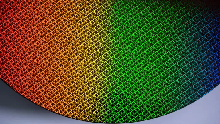
- US Manufacturing: Fab 52 in Arizona is successfully running its first wafer lots, bolstering supply chain security and demonstrating domestic capacity for leading-edge 2nm-class technology.
- Roadmap Ahead: Intel 14A, the successor, is already engaging lead customers with early Process Design Kits (PDKs) and targets risk production in 2027, featuring second-gen RibbonFET/PowerVia.
🏆 Final Verdict
Intel 18A is not merely an incremental node; it is a declaration of war. By pioneering Backside Power Delivery (PowerVia) and integrating RibbonFET, Intel has created a clear architectural advantage in raw performance, validated by early data (2.53 score). However, the race is far from over. While Intel is poised to ship products earlier (Panther Lake in early 2026), TSMC maintains a density lead with N2, and Intel’s execution risk remains high, given past delays. For gamers and consumers, 18A represents the crucial return of competition, promising lower costs and faster innovation in the 2nm class. Its success is the industry’s success, but the final verdict rests on sustained, high-volume yields and cost-effective production over the next 18 months.
Frequently Asked Questions (FAQ)
What is the primary benefit of Intel’s PowerVia?
PowerVia moves power delivery to the back of the wafer, freeing the front side for denser signal routing. This significantly reduces voltage droop (up to 30%) and improves cell utilization by 5-10%, leading to better performance and stability, particularly under heavy load.
When will 18A chips be available to consumers?
The first 18A-based consumer CPUs, Panther Lake (Core Ultra 3-series), are expected to ship before the end of the year, with broad market availability commencing in January 2026.
Is 18A faster than TSMC N2?
Analyst reports suggest Intel 18A holds a lead in raw performance metrics (PPA score of 2.53 vs. N2’s 2.27). However, TSMC N2 is projected to have higher transistor density (313 MTr/mm²), potentially making it more cost-effective for certain die sizes. A definitive comparison awaits production chips.